Variable Shift Register
RTL shift register with parameterizable bit-width and shift length
Created February 2023
Overview
The goal is to create a shift register that can be configured to any specification. This versatile module can be used in many future designs.
A shift register is a daisy chained set of clocked memory elements. With every clock cycle, the input propagates further down the chain, eventually showing at the output. A shift register of length n would take n clock cycles for the input to appear at the output.
Extending this, each memory element could also store multiple bits. If length is the number of chained memories, then width is the number of bits each memory stores.
Given this, we want to make the module's length and width variable.
Design
First we declare the module, its parameters, and IO. We need ports for input, output, and the clock.
Both LENGTH and WIDTH are needed to parameterize our module during instantiation.
// A LENGTH long chain of DFFs WIDTH bits wide
module variable_shift_register #(
    parameter LENGTH = -1,  // LENGTH = # Clk cycles delayed, # of DFFs chained together
    parameter WIDTH = -1    // WIDTH = # Bits wide
    )(
    input clk,
    input [WIDTH-1:0] shift_in,
    output reg [WIDTH-1:0] shift_out
    );

    ...

endmodule
Next, we define an array of registers, each of which is WIDTH bits wide.
// Array of registers
reg [WIDTH-1:0] shift_reg [LENGTH-1:0];
Here, we define the "shift" behavior at every positive edge of the clock.
The current input value is placed into the array's first index. Similarly, the array's last index is assigned to the output.
The for then iteratively moves each register's value to the next register. The "shift" behavior described in this loop will occur simultaneously in parallel.
integer i;
always @(posedge clk) begin
    shift_reg[0] <= shift_in;           // Initial (input) shift
    for (i=0; i<LENGTH-1; i=i+1) begin
        shift_reg[i+1] <= shift_reg[i]; // Iterative shift
    end
    shift_out <= shift_reg[LENGTH-1];   // Final (output) shift
end
Finally, we add in an edge case handling a LENGTH of zero instantiation.
always @(posedge clk) begin
    if (LENGTH==0) begin
        shift_out <= shift_in;  // Just act like a wire and pass along
    end else begin
        ... // Normal shift behavior
    end
end
This is the final implementation.
// A LENGTH long chain of DFFs WIDTH bits wide
module variable_shift_register #(
    parameter LENGTH = -1,  // LENGTH = # Clk cycles delayed, # of dff chained together
    parameter WIDTH = -1    // WIDTH = # Bits wide
    )(
    input clk,
    input [WIDTH-1:0] shift_in,
    output reg [WIDTH-1:0] shift_out
    );

    // Array of registers
    reg [WIDTH-1:0] shift_reg [LENGTH-1:0];

    integer i;
    always @(posedge clk) begin
        if (LENGTH==0) begin
            shift_out <= shift_in;  // Just act like a wire and pass along
        end else begin
            shift_reg[0] <= shift_in;           // Initial (input) shift
            for (i=0; i<LENGTH-1; i=i+1) begin
                shift_reg[i+1] <= shift_reg[i]; // Iterative shift
            end
            shift_out <= shift_reg[LENGTH-1];   // Final (output) shift
        end
    end
endmodule
Testbench
First we declare the module and create IO for the DUT (design under test).
`timescale 1ns / 1ps

module testbench ();

    localparam len = ...;
    localparam wid = ...;
    // IO
    reg [wid-1:0] in;
    wire [wid-1:0] out;

    ...

endmodule
We create a clock with a 10ns period, that starts high and finishes at 100ns.
// Create clock
localparam PERIOD = 10;
reg clk = 1'b1;
always
    #(PERIOD/2) clk = ~clk;
initial
    #100 $finish();
Instantiate the design under test: pass parameters and connect IO.
// Instantiate
variable_shift_register #(
    .LENGTH(len),
    .WIDTH(wid)
) sr_inst (
    .clk(clk),
    .shift_in(in),
    .shift_out(out)
);
Finally create an inital block to drive input signals.
initial begin
    ...     // Set test input at time intervals
end
This testbench instantiates the final design, provides test IO signals.
`timescale 1ns / 1ps

module testbench ();

    localparam len = ...;
    localparam wid = ...;
    // IO
    reg [wid-1:0] in;
    wire [wid-1:0] out;

    // Create clock
    localparam PERIOD = 10;
    reg clk = 1'b1;
    always
        #(PERIOD/2) clk = ~clk;
    initial
        #100 $finish();

    // Instantiate
    variable_shift_register #(
        .LENGTH(len),
        .WIDTH(wid)
    ) sr_inst (
        .clk(clk),
        .shift_in(in),
        .shift_out(out)
    );

    initial begin
        ...     // Set test input at time intervals
    end

endmodule
Results
Each test case below consists of instantiation parameters, the test vector, and the resulting waveform.
The clock is at the top of each waveform, followed by the input to the DUT and it's output. Each bit of a given signal is indexed underneath its integer representation.
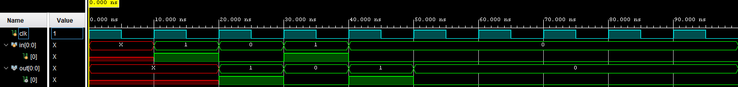
// Test case 1
First we instantiate a 1 bit shift register with a length of 1 (1x1). This instantiation is just a typical flip flop, clocking input to output each cycle.
localparam len = 1;
localparam wid = 1;
One clock cycle after the simulation begins, we set the design's input. Each clock cycle a new value is clocked in: 1, 0, 1, 0.
initial begin
    #(PERIOD) in = 1;
    #(PERIOD) in = 0;
    #(PERIOD) in = 1;
    #(PERIOD) in = 0;
end
This is the resulting waveform. We can see that the input appears at the output with a one cycle delay.
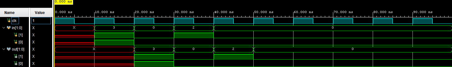
// Test case 2
Now with a bit width of two, we demonstrate a multibit shift register instantiation.
localparam len = 1;
localparam wid = 2;
We send 3 (11), 0 (00), 2 (10), 0 (00) and expect typical flip flop behavior since the length is still one.
initial begin
    #(PERIOD) in = 3;
    #(PERIOD) in = 0;
    #(PERIOD) in = 2;
    #(PERIOD) in = 0;
end
Again, we can see that the input appears at the output with a one cycle delay, this time with multiple bits.
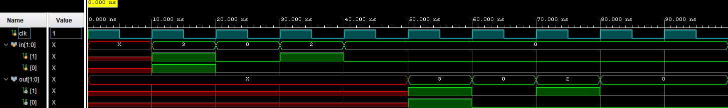
// Test case 3
With the same test vector and bit width, the shift register's length is changed to 4.
localparam len = 4;
localparam wid = 2;
initial begin
#(PERIOD) in = 3;
#(PERIOD) in = 0;
#(PERIOD) in = 2;
#(PERIOD) in = 0;
endWe can see that the resulting waveform is the same as test case 2, but with the output shifted by 4 clock cycles instead of 1.
Conslusion
The final design embodies a shift register that can be instantiated to any specified bit width and shift length.
In general, a shift register of length l will delay it's output by l clock cycles.
Digital designers can utilize shift registers to align data computed at different points in time.
An example of this use case is this Ripple Carry Adder project.